
See what people are saying
README
eSpDR: 80 Msps ESP32-S3 SDR
eSpDR (ESP + SDR) streams raw baseband IQ from an ESP32-S3 radio to a Linux
host at 80 Msps, with lossless compression and end-to-end integrity checks.
Its host tool, iqstream, handles capture, receiver control and the live web
frontend.
ESP32-S3 ADC ──16 GPIO lines──▶ Alchitry Au FPGA ──FT600 USB 3──▶ host
80 Msps, 20-bit IQ pairs        reorder, lossless compression,     parallel decoding,
2 × 8-bit lanes, 240 MHz        256 MiB DDR3 buffer                verification, output
- 80 million IQ pairs per second, I and Q as 10-bit two's complement, centred on a 2440 MHz LO (a sampled span of 2400–2480 MHz). The analog response is not flat across that span, and out-of-band signals can alias into it. The raw ESP convention is LO minus RF for I+jQ.
- The whole stream is checked: every compressed record carries a CRC, and at the end the pair counts and a whole-stream CRC are reconciled across the ESP, the FPGA and the host. If the FPGA ever fails to receive a link unit (about 190 µs of samples), the stream continues and the loss is reported as an exact gap in sample time.
- Typical over-the-air input compresses to about 1.2 bytes per pair, around 95–100 MB/s. The USB path sustains about 190 MB/s. Incompressible input needs 202.5 MB/s including record headers; the 256 MiB DDR buffer absorbs about 20 s of it, or about 2.5 s of a completely stalled host at typical rates. Any lost samples are counted and reported.
- Receive only.
iqstream serveshows a live spectrum and waterfall in a web browser, with receiver controls, live stream counters and DDR buffer usage.
About this project
This project is a technical capability proof of concept and a starting point for further tinkering. Most of the implementation ideas and the system architecture are mine. All original project code was written by AI: GPT 6 Astra and Opus 5.5 took turns over about two weeks, with my direct guidance and supervision. The entire web frontend was one-shotted by Opus 5.5 with the prompt "make an SDR#-inspired WebGL-based web frontend." Getting the actual acquisition working took much longer.
How it works
For the radio details, see Inside the eSpDR receiver: how the hardware supplies I/Q, PLL tuning, sample rates, filters, gain and DC/IQ correction, with results from the development measurements.
The radio IQ path
The samples come from the Wi-Fi/Bluetooth radio's internal receive path after RF downconversion. The selected radio dump format supplies signed 10-bit I and 10-bit Q. An undocumented hardware sample-dump engine writes those pairs directly to internal SRAM.
The supported dump rates are 80 million IQ pairs/s and 16 million IQ
pairs/s (rate=80 and rate=16). Radio configuration and capture live in
radio.c and capture.c.
Four SRAM banks and two CPU-driven output lanes
The dump engine stores each pair in a 32-bit word: I in bits 0–9, Q in bits 10–19, with the remaining bits unused. At 80 Msps that is 320 MB/s entering SRAM. To keep acquisition running while completed samples are sent, the firmware rotates through four 64 KiB banks holding 16,384 pairs each. Core 0 services banks 0 and 2; core 1 services banks 1 and 3. They switch the writer to the next bank before the current bank fills, locate the exact sample boundaries, and send the completed unit while acquisition continues in another bank.
Getting the samples out takes both cores, running bare metal at 240 MHz.
Each bit-bangs an eight-bit dedicated-GPIO lane using wur.gpio_out, giving
16 data wires in total. Both cores handle acquisition control, polling,
packing, checksums and output. Espressif's
dedicated GPIO documentation
explains how these CPU instructions bypass ordinary memory-mapped GPIO access.
Packing and the bandwidth budget
The 320 MB/s SRAM format exceeds the GPIO link's 240 MB/s ceiling, so the
firmware packs each pair down to its 20 useful bits. The assembly kernel in
transmit.S uses the S3's 128-bit SIMD instructions
to pack 16 IQ pairs into 40 bytes, bringing the payload down to 200 MB/s.
Each group contains 32 bytes of low 16-bit values plus eight bytes holding
the remaining four bits of each pair. Loads, packing and
checksum accumulation are interleaved with the GPIO writes.
| Quantity | Rate at nominal 80 Msps |
|---|---|
| Unpacked SRAM words: 4 bytes per IQ pair | 320 MB/s |
| Packed IQ payload: 2.5 bytes per pair | 200 MB/s |
| Absolute maximum GPIO data rate: 240 MHz × 2 cores × 8 bits/core / 2 instructions/sample | 240 MB/s |
| Two-lane packing loop: 40 bytes per 91 CPU cycles per lane | about 211 MB/s, before framing and bank-service overhead |
| FPGA raw-fallback records: 2,560 payload bytes + 32-byte header per 1,024 pairs | 202.5 MB/s |
The packing loop's rate follows from 2 × 240 MHz × 40 / 91. Each complete
link unit also includes time for markers, headers, trailers, fragment transitions
and bank preparation. protocol/link.h defines the layout and
cadence shared by the ESP and FPGA.
Memory placement and link timing
That throughput uses all 16 fast GPIO lanes available through the CPU's
wur.gpio_out register interface for data. Independent ESP and FPGA clocks
would let the sampling point drift across pin transitions. The ESP therefore
forwards a continuous 20 MHz I2S master clock on GPIO41 to the FPGA, while
its own RF and CPU clocks remain referenced to its native 40 MHz crystal.
I2S generates the clock in hardware on a spare GPIO; neither CPU writes an
extra register for each edge.
The FPGA derives its 240 MHz sampler and 120 MHz acquisition pipeline from that input. It follows the firmware's exact instruction timings, starting from a unit marker, and samples between pin transitions. Each byte is normally held for two CPU cycles, with fixed gaps for packing and unit boundaries. Calibrating the sampling phase accounts for the delays in the wiring. Management, DDR and FT600 retain independent clocks, with asynchronous FIFOs at the boundaries. See Clock and bus synchronization.
Instruction and data fetch stalls break that fixed schedule and throw the bus
out of synchronisation. Testing established that SRAM bank separation is
required for both code and data accessed on the timed path. Bank contention
caused stalls with unpredictable frequency and position within the buffer;
in one observed case, a data access on one core stalled an instruction fetch
on the other. Each core therefore runs its own transmit kernel from a separate
bank, with data placement arranged to avoid contention during transmission.
memory.ld fixes those kernel addresses and reserves the
capture memory. Shared control state is handled outside the transmit kernel.
Fitting the stream through USB
The packed stream, with record headers, is 202.5 MB/s, while the USB path sustains about 190 MB/s. The FPGA checks and reorders the two lanes, then losslessly compresses the samples before writing them to its DDR ring. Typical over-the-air input comes down to 95–100 MB/s. The 256 MiB ring absorbs bursts of incompressible data and pauses in host reads while the FT600 drains it over USB. The host decodes the records and checks their CRCs, pair counts and whole-stream CRC against the ESP and FPGA totals.
RF tuning
Tuning to a new frequency also requires selecting a suitable VCO capacitor setting so the PLL can lock. The firmware sets the frequency word, scans all 512 capacitor codes, and picks the middle of the longest interval reporting lock. The capacitor bank tunes the VCO's operating range, and the PLL's frequency-divider feedback sets the frequency.
Bench work found a lock range of roughly 2.2–2.8 GHz in the tested configuration. The current UI accepts 2210–2790 MHz; a failed lock restores the previous LO. The receiver settings and screenshots below include the upper-limit capture from this board.
Hardware
- Alchitry Au (Artix-7 XC7A35T, 256 MiB DDR3) with the Ft (FTDI FT600) and Br (breakout) boards stacked.
- ESP32-S3-WROOM-1 development board with two USB ports: native USB (USB Serial/JTAG) and a "COM" USB-UART bridge whose RTS/DTR drive EN/BOOT. Both connect to the host, as do the Au and the Ft.
- The FT600 must be configured once (FTDI's FT60X Chip Configuration Programmer) for 245 FIFO mode, 1 IN channel, 100 MHz clock.
Wiring
Link lines (ESP GPIO → FPGA ball). Lane 0 is driven by CPU core 0, lane 1 by core 1. Use short, direct wires and a common ground (Br SV4.2 / SV4.20).
| Lane.bit | ESP GPIO | FPGA | Lane.bit | ESP GPIO | FPGA | |
|---|---|---|---|---|---|---|
| 0.0 | 4 | T15 | 1.0 | 3 | P5 | |
| 0.1 | 5 | T14 | 1.1 | 46 | M5 | |
| 0.2 | 6 | P14 | 1.2 | 9 | L4 | |
| 0.3 | 7 | R16 | 1.3 | 10 | P4 | |
| 0.4 | 15 | M15 | 1.4 | 11 | N3 | |
| 0.5 | 16 | R15 | 1.5 | 12 | R10 | |
| 0.6 | 17 | L5 | 1.6 | 13 | R12 | |
| 0.7 | 18 | N4 | 1.7 | 14 | R13 |
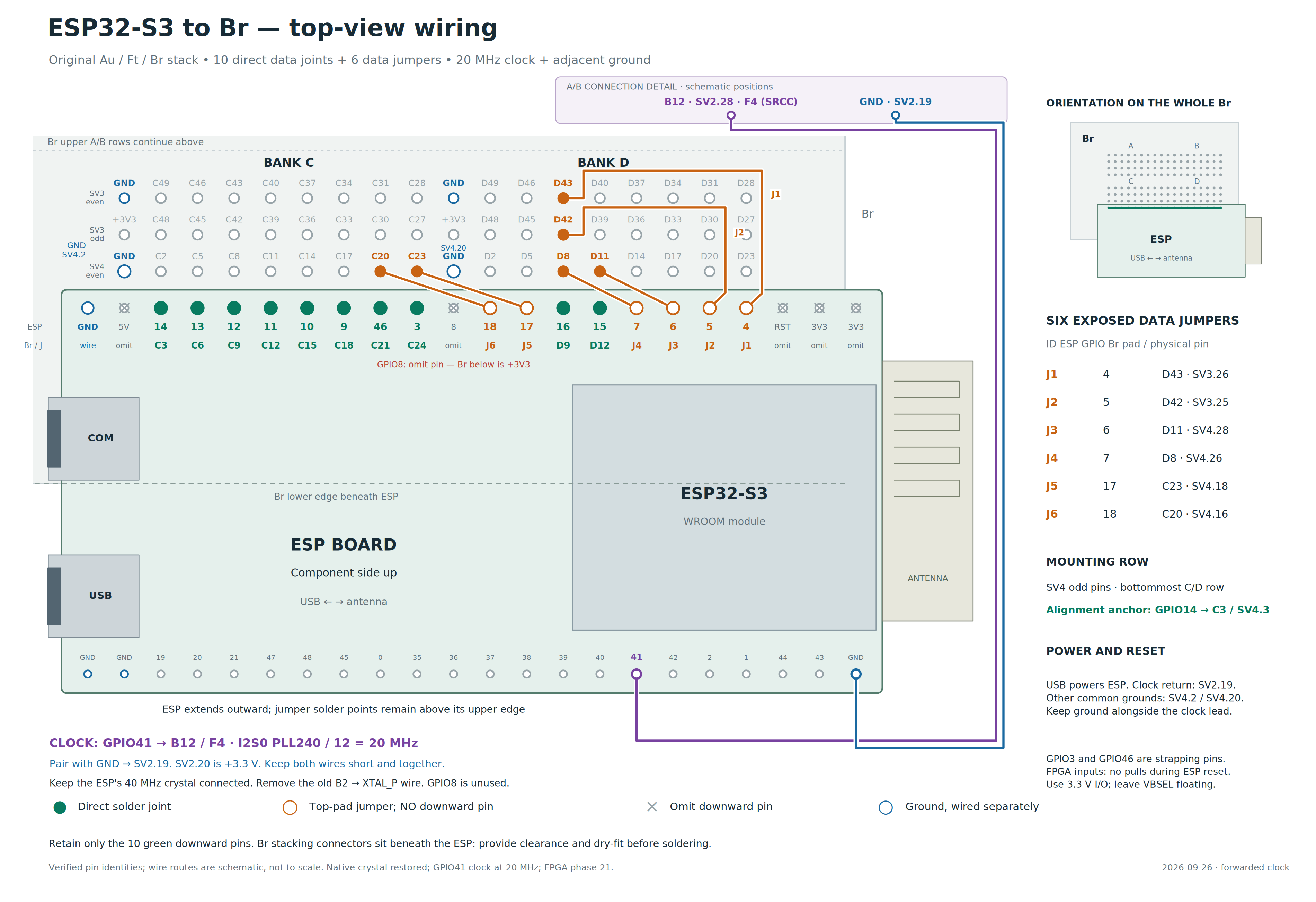
Open the zoomable wiring diagram. It shows all sixteen data connections and the clock/ground pair.
Forwarded clock. Keep the ESP's native crystal connected. Connect ESP GPIO41 → Br B12 → FPGA F4 (clock-capable SRCC input, SV2 pin 28). Route an ESP ground wire alongside it to Br SV2 pin 19 (GND); pin 20 is +3.3 V. The clock passes through connector B, separately from the C/D data wiring. The firmware generates 20 MHz using I2S0 MCLK, PLL240 divided by 12, with 10 mA drive. All sixteen data pads also use 10 mA.
If upgrading the earlier wiring, remove the Br B2/D1 → XTAL_P wire and restore the crystal's series connection (R4 on the modified WROOM-1 module). The FPGA no longer drives that pad. GPIO8 was an intermediate clock experiment; it is unused in this topology and its downward pin must remain omitted because the Br pad beneath it is +3.3 V.
The selected FPGA sampling phase is 21, with the existing per-line input
delays and rising-edge data sampling. It passed a 30-minute 80 Msps run with
zero integrity errors on this assembly. Wiring changes require recalibration:
run iqstream calibrate and verify the intended rate. The detailed topology,
startup sequence and clock-fault handling are in CLOCK-SYNC.md.
Building
Each part builds on its own:
| Part | Requires | Command | Output |
|---|---|---|---|
| ESP32-S3 firmware | ESP-IDF v5.5 (. $IDF_PATH/export.sh) | make -C esp32s3 | esp32s3/build/iq-source.bin |
| FPGA image | Vivado 2025.2 (vivado on PATH, or VIVADO=...) | fpga/build.sh (about 30 min) | fpga/build/iqstream.bit |
| Host tool | C++17, zlib, FFTW3 single precision (libfftw3-dev), FTDI D3XX for Linux | make -C host D3XX_DIR=/path/to/d3xx | host/build/iqstream |
| Tests | C++17, zlib, FFTW3, Verilator 5 | tests/run.sh (--long adds a full-size run) | pass/fail |
From the repository root, add the built host tool to your shell's PATH for
the commands below:
export PATH="$PWD/host/build:$PATH"
The FPGA build fails unless every timing constraint is met. The firmware build fails if any of its functions would be shadowed by a same-named ROM function.
Loading also needs openFPGALoader and esptool.py (part of ESP-IDF) on
PATH, or set OPENFPGALOADER / ESPTOOL, for example
ESPTOOL="python -m esptool". The user needs access to the serial ports and
the FT600 (udev rules for 0403:601e).
Running
Load both devices into RAM. A power cycle restores the boards.
iqstream load --fpga fpga/build/iqstream.bit --esp esp32s3/build/iq-source.bin
This holds the ESP in reset, loads the FPGA and waits for its management and
DDR domains. It then boots the ESP from its crystal into the ROM loader and
loads the RAM firmware. After radio initialization, the ESP starts its 20 MHz
clock output; the host waits for FPGA clock lock, sampling phase and input-delay
readiness. Repeat after any power cycle. To reload only the ESP, drop --fpga;
the matching FPGA image must already be loaded.
Capture:
iqstream capture --seconds 10                         # verify only
iqstream capture --seconds 60 --output capture.iqc    # compressed records (~1.2 B/pair)
iqstream capture --seconds 5 --output capture.cs16    # int16 I, Q (4 B/pair)
iqstream capture --seconds 0 --output - | consumer    # until Ctrl-C, to stdout
capture prints progress, then a summary. Exit status:
| Status | Meaning |
|---|---|
| 0 | every pair received, decoded and matched against the ESP's and the FPGA's counts and CRCs |
| 3 | complete, but some link units were lost: the summary gives the number of gaps and pairs; every delivered pair is verified and indices (and .cs16 output) keep sample time |
| 1 | failed; the summary lists what did not reconcile |
The summary and progress go to stderr, so --output - can feed a pipe.
When a consumer falls behind, it back-pressures USB. The FPGA's 256 MiB DDR
buffer holds the incoming samples until the host catches up or the buffer fills.
The FPGA carries one stream at a time. A capture opens it and closes it when it
finishes, and while it is open the FPGA refuses to start another. Only one
iqstream process can use the devices at once. If a capture is killed, the
next capture closes the stream it left open and says so.
Other commands:
iqstream decode capture.iqc capture.cs16   # .iqc to interleaved int16
iqstream status                            # identities, readiness, receiver settings, last-run counters
iqstream set lo=2426M gain=40              # change receiver settings (below)
iqstream calibrate                         # measure the link sampling window, use its centre
calibrate streams for one second at every fourth sampling phase across the
full 240 MHz period (a few minutes), reports the window without link errors
and sets the FPGA to its centre until the FPGA is reloaded. Reuse the measured
phase with iqstream load ... --phase P, or set DEFAULT_PHASE and rebuild.
There are 224 phase positions per 240 MHz period, about 18.6 ps per step;
the default for the qualified assembly is 21.
Devices are found automatically in /dev/serial/by-id and by FT600 serial
number. With several boards attached, choose with --esp-port, --fpga-port,
--com-port, --ftdi-serial and --ft600.
Receiver settings
The ESP boots with the LO at 2440 MHz, gain selector 24, 80 Msps, 40 MHz
analog width, RC filter code 0 and everything else automatic. iqstream set
(or the browser) changes them; they last until the ESP is reloaded, and
status shows them. Each change reconfigures the whole receive path, so it
is made between captures.
| Setting | Values | Notes |
|---|---|---|
lo= | 2210–2790 MHz (2402M, 2.44G, Hz) | Steps of 457.76 Hz; the exact LO is reported. A failed PLL lock keeps the previous LO |
rate= | 80, 16 | Msps; the spectrum spans the sample rate |
width= | 40, 20 | Analog channel width, MHz |
filter= | N or N,M, 0–63 | Baseband RC filter codes of the width's register pair; higher is narrower, 0 widest |
gain= | 0–127 | A gain-table index, not dB: about 1 dB a step from 35 to 76; 83 and up repeat the low end. Sets both gain stages |
rf=, bb= | 0–511, 0–127, or auto | The RF and baseband gain stages directly, overriding the table |
dc0=…dc3= | 0–511 or auto | DC offset: 0, 1 shift I and 2, 3 shift Q, by about 1.2 and 0.8 ADC counts a code |
iq= | A,P or auto | I/Q correction: amplitude −16…15 (about 1/64 a step), phase −32…31 (about 1/128) |
auto keeps the vendor calibration or the gain table's value.
Live spectrum in a browser
iqstream serve                              # http://127.0.0.1:8073/
iqstream serve --listen 0.0.0.0:8073        # reachable from other machines
Open the address in a browser with WebGL 2 support. From a
remote workstation, forward the port (ssh -L 8073:127.0.0.1:8073 host, or
the editor's port forwarding) rather than listening on every interface: the
page controls the receiver and has no login.
The page is modelled on SDR#: the LO in large digits (scroll or click a digit; press Enter or type to enter a frequency), a spectrum over a waterfall, and Zoom, Contrast, Range and Offset beside them. Wheel or pinch to zoom, drag to pan, click for a marker, right-click to remove it, double-click to tune there. The side panels hold:
- Receiver: every setting above.
- FFT: resolution, window, speed (frames per second), averaging and detector. The defaults are SDR#'s: 4096 points, Blackman-Harris 4, 40 frames a second, one block per frame; peak detection over more blocks shows short bursts such as Bluetooth advertisements. Levels are dBFS: a full-scale tone reads 0.
- Display: SDR#'s spectrum and waterfall attack and decay, colours, a Bluetooth LE or Wi-Fi channel plan, peak hold. Kept in the browser.
- Stream: the FPGA's DDR buffer (used, free, capacity, peak), throughput and compression, every error counter of the current run as it happens, and the verification result of the last completed run.
- Connection: round trip, frame rate, link use, and limits on frame rate, bandwidth and resolution.
Every run uses the same verification as capture. Changing a receiver setting
ends and verifies the current run, then starts another with the new settings.
Stop ends and verifies the current run and leaves streaming paused. Streaming
also pauses after ten seconds without a browser connected. serve holds the
devices, like any other command: stop it (Ctrl-C) to run capture. If the
devices are not loaded yet, the page says so and serve keeps trying.
One browser is served at a time; opening the page elsewhere takes over, and the first page offers to take it back.
A slow browser connection can turn a queue of spectrum frames into a delayed view of the radio. To keep the display current, the server fits frames to the visible range and screen width, and limits how many can be awaiting an acknowledgement. When the connection falls behind, it merges frames, keeping their peaks in peak mode so short signals still show. Automatic resolution reduces the bins per frame in steps until about 15 frames a second get through. The page reconnects by itself, with the receiver as it was.
Screenshots
Live hardware at 80 Msps, using the maximum 262,144-point FFT and 100 fps setting, with all FFT blocks included, peak detection and DC removal enabled. The overview captures use a 2440 MHz LO and gain selector 25; the display uses a −34 to −101 dBFS scale and Bluetooth LE channel overlays. Click an image to view it at full resolution.
Receiver and FFT controls, with the full 80 MHz span:

Display controls, with the same live receiver and spectrum settings:

Stream statistics, with live throughput, DDR buffer use and integrity counters:

Minimum LO: 2210 MHz, showing the full 80 MHz span:

Upper LO: 2781 MHz, the highest setting that locked during this capture session's 1 MHz checks. This board returned a PLL lock error at 2782–2790 MHz.

Output formats
.cs16: interleaved little-endian int16 I, Q, one pair per 4 bytes, values
−512..511. Lost pairs, if any, are written as zeros so the file keeps
sample time.
.iqc: the FPGA's compressed records, exactly as received, ending with the
END record. Each record holds up to 1024 pairs with its own header CRC and
data CRC; protocol/iq_record.h documents the format, and
protocol/iq_record.cpp is a reference decoder.
Fixed configuration
| Setting | Where |
|---|---|
| Receiver settings at boot (LO 2440 MHz, gain selector 24) | esp32s3/src/radio.h |
| Control protocol, statistics | protocol/control.h |
| Link unit format and timing | protocol/link.h |
| Compressed record format | protocol/iq_record.h |
The FPGA and host build their constants from these headers.
Repository layout
protocol/          shared definitions: control protocol, link format, record format + codec
esp32s3/           ESP32-S3 firmware (bare metal, both cores, RAM image)
fpga/              RTL, constraints, MIG configuration and Vivado build
host/              iqstream host tool; host/web: the browser UI, compiled into it
tests/             codec, spectrum, web server, link-receiver and RTL stream tests
docs/images/       wiring diagram and screenshots used by this README
Local recordings, screenshot originals, demo scripts, posts and measurement
artifacts belong in local/, which is excluded from Git. Selected README images
live in docs/images/. Build outputs are also ignored.
Troubleshooting
... is not running this iqstream's ESP firmware(or FPGA image): the host tool, the firmware and the FPGA image are built together from one tree; load the images built with this host tool.FPGA not ready: !esp-clock(or!phase,!deskew,!ddr): runiqstream loadwith matching images. Check the restored crystal and the GPIO41 → B12 clock/ground pair. The forwarded clock starts only after ESP firmware initializes the radio.- Forwarded-clock fault or pulse anomalies: the host fails the capture. Check the short clock lead, adjacent ground and 10 mA drive. Management and DDR remain independently clocked; load/re-arm only after the source is stable.
- Gaps (exit status 3), ESP acquisition failures or lane checksum errors:
check data wiring and ground, then run
iqstream calibrate. MMCM lock alone does not establish a clean data-sampling window. - Reorder overflows: the host stopped reading for longer than the DDR
buffer covers (a few seconds at typical rates), so samples were dropped at
the FPGA input. Write
.iqcrather than.cs16, use a faster disk, or check that the FT600 is on a USB 3 port.
License
Original eSpDR code is released under the Zero-Clause BSD license (0BSD). You can use, modify and distribute that code for any purpose, including commercially, without an attribution requirement.
Third-party code and dependencies retain their respective licenses, including
Espressif's Apache-2.0 PHY library
and the MIT-licensed startup vectors in
vectors.S. Redistributed firmware must include the
licenses and notices required by the components it contains.
Similar repos


Languages
C++
36.4%
Verilog
30.7%
C
11.8%
JavaScript
10.7%
Assembly
2.5%
Tcl
1.9%
HTML
1.8%
CSS
1.5%
Makefile
1.2%
Shell
1.1%
See what people are saying
README
eSpDR: 80 Msps ESP32-S3 SDR
eSpDR (ESP + SDR) streams raw baseband IQ from an ESP32-S3 radio to a Linux
host at 80 Msps, with lossless compression and end-to-end integrity checks.
Its host tool, iqstream, handles capture, receiver control and the live web
frontend.
ESP32-S3 ADC ──16 GPIO lines──▶ Alchitry Au FPGA ──FT600 USB 3──▶ host
80 Msps, 20-bit IQ pairs        reorder, lossless compression,     parallel decoding,
2 × 8-bit lanes, 240 MHz        256 MiB DDR3 buffer                verification, output
- 80 million IQ pairs per second, I and Q as 10-bit two's complement, centred on a 2440 MHz LO (a sampled span of 2400–2480 MHz). The analog response is not flat across that span, and out-of-band signals can alias into it. The raw ESP convention is LO minus RF for I+jQ.
- The whole stream is checked: every compressed record carries a CRC, and at the end the pair counts and a whole-stream CRC are reconciled across the ESP, the FPGA and the host. If the FPGA ever fails to receive a link unit (about 190 µs of samples), the stream continues and the loss is reported as an exact gap in sample time.
- Typical over-the-air input compresses to about 1.2 bytes per pair, around 95–100 MB/s. The USB path sustains about 190 MB/s. Incompressible input needs 202.5 MB/s including record headers; the 256 MiB DDR buffer absorbs about 20 s of it, or about 2.5 s of a completely stalled host at typical rates. Any lost samples are counted and reported.
- Receive only.
iqstream serveshows a live spectrum and waterfall in a web browser, with receiver controls, live stream counters and DDR buffer usage.
About this project
This project is a technical capability proof of concept and a starting point for further tinkering. Most of the implementation ideas and the system architecture are mine. All original project code was written by AI: GPT 6 Astra and Opus 5.5 took turns over about two weeks, with my direct guidance and supervision. The entire web frontend was one-shotted by Opus 5.5 with the prompt "make an SDR#-inspired WebGL-based web frontend." Getting the actual acquisition working took much longer.
How it works
For the radio details, see Inside the eSpDR receiver: how the hardware supplies I/Q, PLL tuning, sample rates, filters, gain and DC/IQ correction, with results from the development measurements.
The radio IQ path
The samples come from the Wi-Fi/Bluetooth radio's internal receive path after RF downconversion. The selected radio dump format supplies signed 10-bit I and 10-bit Q. An undocumented hardware sample-dump engine writes those pairs directly to internal SRAM.
The supported dump rates are 80 million IQ pairs/s and 16 million IQ
pairs/s (rate=80 and rate=16). Radio configuration and capture live in
radio.c and capture.c.
Four SRAM banks and two CPU-driven output lanes
The dump engine stores each pair in a 32-bit word: I in bits 0–9, Q in bits 10–19, with the remaining bits unused. At 80 Msps that is 320 MB/s entering SRAM. To keep acquisition running while completed samples are sent, the firmware rotates through four 64 KiB banks holding 16,384 pairs each. Core 0 services banks 0 and 2; core 1 services banks 1 and 3. They switch the writer to the next bank before the current bank fills, locate the exact sample boundaries, and send the completed unit while acquisition continues in another bank.
Getting the samples out takes both cores, running bare metal at 240 MHz.
Each bit-bangs an eight-bit dedicated-GPIO lane using wur.gpio_out, giving
16 data wires in total. Both cores handle acquisition control, polling,
packing, checksums and output. Espressif's
dedicated GPIO documentation
explains how these CPU instructions bypass ordinary memory-mapped GPIO access.
Packing and the bandwidth budget
The 320 MB/s SRAM format exceeds the GPIO link's 240 MB/s ceiling, so the
firmware packs each pair down to its 20 useful bits. The assembly kernel in
transmit.S uses the S3's 128-bit SIMD instructions
to pack 16 IQ pairs into 40 bytes, bringing the payload down to 200 MB/s.
Each group contains 32 bytes of low 16-bit values plus eight bytes holding
the remaining four bits of each pair. Loads, packing and
checksum accumulation are interleaved with the GPIO writes.
| Quantity | Rate at nominal 80 Msps |
|---|---|
| Unpacked SRAM words: 4 bytes per IQ pair | 320 MB/s |
| Packed IQ payload: 2.5 bytes per pair | 200 MB/s |
| Absolute maximum GPIO data rate: 240 MHz × 2 cores × 8 bits/core / 2 instructions/sample | 240 MB/s |
| Two-lane packing loop: 40 bytes per 91 CPU cycles per lane | about 211 MB/s, before framing and bank-service overhead |
| FPGA raw-fallback records: 2,560 payload bytes + 32-byte header per 1,024 pairs | 202.5 MB/s |
The packing loop's rate follows from 2 × 240 MHz × 40 / 91. Each complete
link unit also includes time for markers, headers, trailers, fragment transitions
and bank preparation. protocol/link.h defines the layout and
cadence shared by the ESP and FPGA.
Memory placement and link timing
That throughput uses all 16 fast GPIO lanes available through the CPU's
wur.gpio_out register interface for data. Independent ESP and FPGA clocks
would let the sampling point drift across pin transitions. The ESP therefore
forwards a continuous 20 MHz I2S master clock on GPIO41 to the FPGA, while
its own RF and CPU clocks remain referenced to its native 40 MHz crystal.
I2S generates the clock in hardware on a spare GPIO; neither CPU writes an
extra register for each edge.
The FPGA derives its 240 MHz sampler and 120 MHz acquisition pipeline from that input. It follows the firmware's exact instruction timings, starting from a unit marker, and samples between pin transitions. Each byte is normally held for two CPU cycles, with fixed gaps for packing and unit boundaries. Calibrating the sampling phase accounts for the delays in the wiring. Management, DDR and FT600 retain independent clocks, with asynchronous FIFOs at the boundaries. See Clock and bus synchronization.
Instruction and data fetch stalls break that fixed schedule and throw the bus
out of synchronisation. Testing established that SRAM bank separation is
required for both code and data accessed on the timed path. Bank contention
caused stalls with unpredictable frequency and position within the buffer;
in one observed case, a data access on one core stalled an instruction fetch
on the other. Each core therefore runs its own transmit kernel from a separate
bank, with data placement arranged to avoid contention during transmission.
memory.ld fixes those kernel addresses and reserves the
capture memory. Shared control state is handled outside the transmit kernel.
Fitting the stream through USB
The packed stream, with record headers, is 202.5 MB/s, while the USB path sustains about 190 MB/s. The FPGA checks and reorders the two lanes, then losslessly compresses the samples before writing them to its DDR ring. Typical over-the-air input comes down to 95–100 MB/s. The 256 MiB ring absorbs bursts of incompressible data and pauses in host reads while the FT600 drains it over USB. The host decodes the records and checks their CRCs, pair counts and whole-stream CRC against the ESP and FPGA totals.
RF tuning
Tuning to a new frequency also requires selecting a suitable VCO capacitor setting so the PLL can lock. The firmware sets the frequency word, scans all 512 capacitor codes, and picks the middle of the longest interval reporting lock. The capacitor bank tunes the VCO's operating range, and the PLL's frequency-divider feedback sets the frequency.
Bench work found a lock range of roughly 2.2–2.8 GHz in the tested configuration. The current UI accepts 2210–2790 MHz; a failed lock restores the previous LO. The receiver settings and screenshots below include the upper-limit capture from this board.
Hardware
- Alchitry Au (Artix-7 XC7A35T, 256 MiB DDR3) with the Ft (FTDI FT600) and Br (breakout) boards stacked.
- ESP32-S3-WROOM-1 development board with two USB ports: native USB (USB Serial/JTAG) and a "COM" USB-UART bridge whose RTS/DTR drive EN/BOOT. Both connect to the host, as do the Au and the Ft.
- The FT600 must be configured once (FTDI's FT60X Chip Configuration Programmer) for 245 FIFO mode, 1 IN channel, 100 MHz clock.
Wiring
Link lines (ESP GPIO → FPGA ball). Lane 0 is driven by CPU core 0, lane 1 by core 1. Use short, direct wires and a common ground (Br SV4.2 / SV4.20).
| Lane.bit | ESP GPIO | FPGA | Lane.bit | ESP GPIO | FPGA | |
|---|---|---|---|---|---|---|
| 0.0 | 4 | T15 | 1.0 | 3 | P5 | |
| 0.1 | 5 | T14 | 1.1 | 46 | M5 | |
| 0.2 | 6 | P14 | 1.2 | 9 | L4 | |
| 0.3 | 7 | R16 | 1.3 | 10 | P4 | |
| 0.4 | 15 | M15 | 1.4 | 11 | N3 | |
| 0.5 | 16 | R15 | 1.5 | 12 | R10 | |
| 0.6 | 17 | L5 | 1.6 | 13 | R12 | |
| 0.7 | 18 | N4 | 1.7 | 14 | R13 |
Open the zoomable wiring diagram. It shows all sixteen data connections and the clock/ground pair.
Forwarded clock. Keep the ESP's native crystal connected. Connect ESP GPIO41 → Br B12 → FPGA F4 (clock-capable SRCC input, SV2 pin 28). Route an ESP ground wire alongside it to Br SV2 pin 19 (GND); pin 20 is +3.3 V. The clock passes through connector B, separately from the C/D data wiring. The firmware generates 20 MHz using I2S0 MCLK, PLL240 divided by 12, with 10 mA drive. All sixteen data pads also use 10 mA.
If upgrading the earlier wiring, remove the Br B2/D1 → XTAL_P wire and restore the crystal's series connection (R4 on the modified WROOM-1 module). The FPGA no longer drives that pad. GPIO8 was an intermediate clock experiment; it is unused in this topology and its downward pin must remain omitted because the Br pad beneath it is +3.3 V.
The selected FPGA sampling phase is 21, with the existing per-line input
delays and rising-edge data sampling. It passed a 30-minute 80 Msps run with
zero integrity errors on this assembly. Wiring changes require recalibration:
run iqstream calibrate and verify the intended rate. The detailed topology,
startup sequence and clock-fault handling are in CLOCK-SYNC.md.
Building
Each part builds on its own:
| Part | Requires | Command | Output |
|---|---|---|---|
| ESP32-S3 firmware | ESP-IDF v5.5 (. $IDF_PATH/export.sh) | make -C esp32s3 | esp32s3/build/iq-source.bin |
| FPGA image | Vivado 2025.2 (vivado on PATH, or VIVADO=...) | fpga/build.sh (about 30 min) | fpga/build/iqstream.bit |
| Host tool | C++17, zlib, FFTW3 single precision (libfftw3-dev), FTDI D3XX for Linux | make -C host D3XX_DIR=/path/to/d3xx | host/build/iqstream |
| Tests | C++17, zlib, FFTW3, Verilator 5 | tests/run.sh (--long adds a full-size run) | pass/fail |
From the repository root, add the built host tool to your shell's PATH for
the commands below:
export PATH="$PWD/host/build:$PATH"
The FPGA build fails unless every timing constraint is met. The firmware build fails if any of its functions would be shadowed by a same-named ROM function.
Loading also needs openFPGALoader and esptool.py (part of ESP-IDF) on
PATH, or set OPENFPGALOADER / ESPTOOL, for example
ESPTOOL="python -m esptool". The user needs access to the serial ports and
the FT600 (udev rules for 0403:601e).
Running
Load both devices into RAM. A power cycle restores the boards.
iqstream load --fpga fpga/build/iqstream.bit --esp esp32s3/build/iq-source.bin
This holds the ESP in reset, loads the FPGA and waits for its management and
DDR domains. It then boots the ESP from its crystal into the ROM loader and
loads the RAM firmware. After radio initialization, the ESP starts its 20 MHz
clock output; the host waits for FPGA clock lock, sampling phase and input-delay
readiness. Repeat after any power cycle. To reload only the ESP, drop --fpga;
the matching FPGA image must already be loaded.
Capture:
iqstream capture --seconds 10                         # verify only
iqstream capture --seconds 60 --output capture.iqc    # compressed records (~1.2 B/pair)
iqstream capture --seconds 5 --output capture.cs16    # int16 I, Q (4 B/pair)
iqstream capture --seconds 0 --output - | consumer    # until Ctrl-C, to stdout
capture prints progress, then a summary. Exit status:
| Status | Meaning |
|---|---|
| 0 | every pair received, decoded and matched against the ESP's and the FPGA's counts and CRCs |
| 3 | complete, but some link units were lost: the summary gives the number of gaps and pairs; every delivered pair is verified and indices (and .cs16 output) keep sample time |
| 1 | failed; the summary lists what did not reconcile |
The summary and progress go to stderr, so --output - can feed a pipe.
When a consumer falls behind, it back-pressures USB. The FPGA's 256 MiB DDR
buffer holds the incoming samples until the host catches up or the buffer fills.
The FPGA carries one stream at a time. A capture opens it and closes it when it
finishes, and while it is open the FPGA refuses to start another. Only one
iqstream process can use the devices at once. If a capture is killed, the
next capture closes the stream it left open and says so.
Other commands:
iqstream decode capture.iqc capture.cs16   # .iqc to interleaved int16
iqstream status                            # identities, readiness, receiver settings, last-run counters
iqstream set lo=2426M gain=40              # change receiver settings (below)
iqstream calibrate                         # measure the link sampling window, use its centre
calibrate streams for one second at every fourth sampling phase across the
full 240 MHz period (a few minutes), reports the window without link errors
and sets the FPGA to its centre until the FPGA is reloaded. Reuse the measured
phase with iqstream load ... --phase P, or set DEFAULT_PHASE and rebuild.
There are 224 phase positions per 240 MHz period, about 18.6 ps per step;
the default for the qualified assembly is 21.
Devices are found automatically in /dev/serial/by-id and by FT600 serial
number. With several boards attached, choose with --esp-port, --fpga-port,
--com-port, --ftdi-serial and --ft600.
Receiver settings
The ESP boots with the LO at 2440 MHz, gain selector 24, 80 Msps, 40 MHz
analog width, RC filter code 0 and everything else automatic. iqstream set
(or the browser) changes them; they last until the ESP is reloaded, and
status shows them. Each change reconfigures the whole receive path, so it
is made between captures.
| Setting | Values | Notes |
|---|---|---|
lo= | 2210–2790 MHz (2402M, 2.44G, Hz) | Steps of 457.76 Hz; the exact LO is reported. A failed PLL lock keeps the previous LO |
rate= | 80, 16 | Msps; the spectrum spans the sample rate |
width= | 40, 20 | Analog channel width, MHz |
filter= | N or N,M, 0–63 | Baseband RC filter codes of the width's register pair; higher is narrower, 0 widest |
gain= | 0–127 | A gain-table index, not dB: about 1 dB a step from 35 to 76; 83 and up repeat the low end. Sets both gain stages |
rf=, bb= | 0–511, 0–127, or auto | The RF and baseband gain stages directly, overriding the table |
dc0=…dc3= | 0–511 or auto | DC offset: 0, 1 shift I and 2, 3 shift Q, by about 1.2 and 0.8 ADC counts a code |
iq= | A,P or auto | I/Q correction: amplitude −16…15 (about 1/64 a step), phase −32…31 (about 1/128) |
auto keeps the vendor calibration or the gain table's value.
Live spectrum in a browser
iqstream serve                              # http://127.0.0.1:8073/
iqstream serve --listen 0.0.0.0:8073        # reachable from other machines
Open the address in a browser with WebGL 2 support. From a
remote workstation, forward the port (ssh -L 8073:127.0.0.1:8073 host, or
the editor's port forwarding) rather than listening on every interface: the
page controls the receiver and has no login.
The page is modelled on SDR#: the LO in large digits (scroll or click a digit; press Enter or type to enter a frequency), a spectrum over a waterfall, and Zoom, Contrast, Range and Offset beside them. Wheel or pinch to zoom, drag to pan, click for a marker, right-click to remove it, double-click to tune there. The side panels hold:
- Receiver: every setting above.
- FFT: resolution, window, speed (frames per second), averaging and detector. The defaults are SDR#'s: 4096 points, Blackman-Harris 4, 40 frames a second, one block per frame; peak detection over more blocks shows short bursts such as Bluetooth advertisements. Levels are dBFS: a full-scale tone reads 0.
- Display: SDR#'s spectrum and waterfall attack and decay, colours, a Bluetooth LE or Wi-Fi channel plan, peak hold. Kept in the browser.
- Stream: the FPGA's DDR buffer (used, free, capacity, peak), throughput and compression, every error counter of the current run as it happens, and the verification result of the last completed run.
- Connection: round trip, frame rate, link use, and limits on frame rate, bandwidth and resolution.
Every run uses the same verification as capture. Changing a receiver setting
ends and verifies the current run, then starts another with the new settings.
Stop ends and verifies the current run and leaves streaming paused. Streaming
also pauses after ten seconds without a browser connected. serve holds the
devices, like any other command: stop it (Ctrl-C) to run capture. If the
devices are not loaded yet, the page says so and serve keeps trying.
One browser is served at a time; opening the page elsewhere takes over, and the first page offers to take it back.
A slow browser connection can turn a queue of spectrum frames into a delayed view of the radio. To keep the display current, the server fits frames to the visible range and screen width, and limits how many can be awaiting an acknowledgement. When the connection falls behind, it merges frames, keeping their peaks in peak mode so short signals still show. Automatic resolution reduces the bins per frame in steps until about 15 frames a second get through. The page reconnects by itself, with the receiver as it was.
Screenshots
Live hardware at 80 Msps, using the maximum 262,144-point FFT and 100 fps setting, with all FFT blocks included, peak detection and DC removal enabled. The overview captures use a 2440 MHz LO and gain selector 25; the display uses a −34 to −101 dBFS scale and Bluetooth LE channel overlays. Click an image to view it at full resolution.
Receiver and FFT controls, with the full 80 MHz span:
Display controls, with the same live receiver and spectrum settings:
Stream statistics, with live throughput, DDR buffer use and integrity counters:
Minimum LO: 2210 MHz, showing the full 80 MHz span:
Upper LO: 2781 MHz, the highest setting that locked during this capture session's 1 MHz checks. This board returned a PLL lock error at 2782–2790 MHz.
Output formats
.cs16: interleaved little-endian int16 I, Q, one pair per 4 bytes, values
−512..511. Lost pairs, if any, are written as zeros so the file keeps
sample time.
.iqc: the FPGA's compressed records, exactly as received, ending with the
END record. Each record holds up to 1024 pairs with its own header CRC and
data CRC; protocol/iq_record.h documents the format, and
protocol/iq_record.cpp is a reference decoder.
Fixed configuration
| Setting | Where |
|---|---|
| Receiver settings at boot (LO 2440 MHz, gain selector 24) | esp32s3/src/radio.h |
| Control protocol, statistics | protocol/control.h |
| Link unit format and timing | protocol/link.h |
| Compressed record format | protocol/iq_record.h |
The FPGA and host build their constants from these headers.
Repository layout
protocol/          shared definitions: control protocol, link format, record format + codec
esp32s3/           ESP32-S3 firmware (bare metal, both cores, RAM image)
fpga/              RTL, constraints, MIG configuration and Vivado build
host/              iqstream host tool; host/web: the browser UI, compiled into it
tests/             codec, spectrum, web server, link-receiver and RTL stream tests
docs/images/       wiring diagram and screenshots used by this README
Local recordings, screenshot originals, demo scripts, posts and measurement
artifacts belong in local/, which is excluded from Git. Selected README images
live in docs/images/. Build outputs are also ignored.
Troubleshooting
... is not running this iqstream's ESP firmware(or FPGA image): the host tool, the firmware and the FPGA image are built together from one tree; load the images built with this host tool.FPGA not ready: !esp-clock(or!phase,!deskew,!ddr): runiqstream loadwith matching images. Check the restored crystal and the GPIO41 → B12 clock/ground pair. The forwarded clock starts only after ESP firmware initializes the radio.- Forwarded-clock fault or pulse anomalies: the host fails the capture. Check the short clock lead, adjacent ground and 10 mA drive. Management and DDR remain independently clocked; load/re-arm only after the source is stable.
- Gaps (exit status 3), ESP acquisition failures or lane checksum errors:
check data wiring and ground, then run
iqstream calibrate. MMCM lock alone does not establish a clean data-sampling window. - Reorder overflows: the host stopped reading for longer than the DDR
buffer covers (a few seconds at typical rates), so samples were dropped at
the FPGA input. Write
.iqcrather than.cs16, use a faster disk, or check that the FT600 is on a USB 3 port.
License
Original eSpDR code is released under the Zero-Clause BSD license (0BSD). You can use, modify and distribute that code for any purpose, including commercially, without an attribution requirement.
Third-party code and dependencies retain their respective licenses, including
Espressif's Apache-2.0 PHY library
and the MIT-licensed startup vectors in
vectors.S. Redistributed firmware must include the
licenses and notices required by the components it contains.
Similar repos
Languages
C++
36.4%
Verilog
30.7%
C
11.8%
JavaScript
10.7%
Assembly
2.5%
Tcl
1.9%
HTML
1.8%
CSS
1.5%
Makefile
1.2%
Shell
1.1%